
A step-by-step guide to assembling a high-performance amplifier in an afternoon for under $50.
What is NS-01?
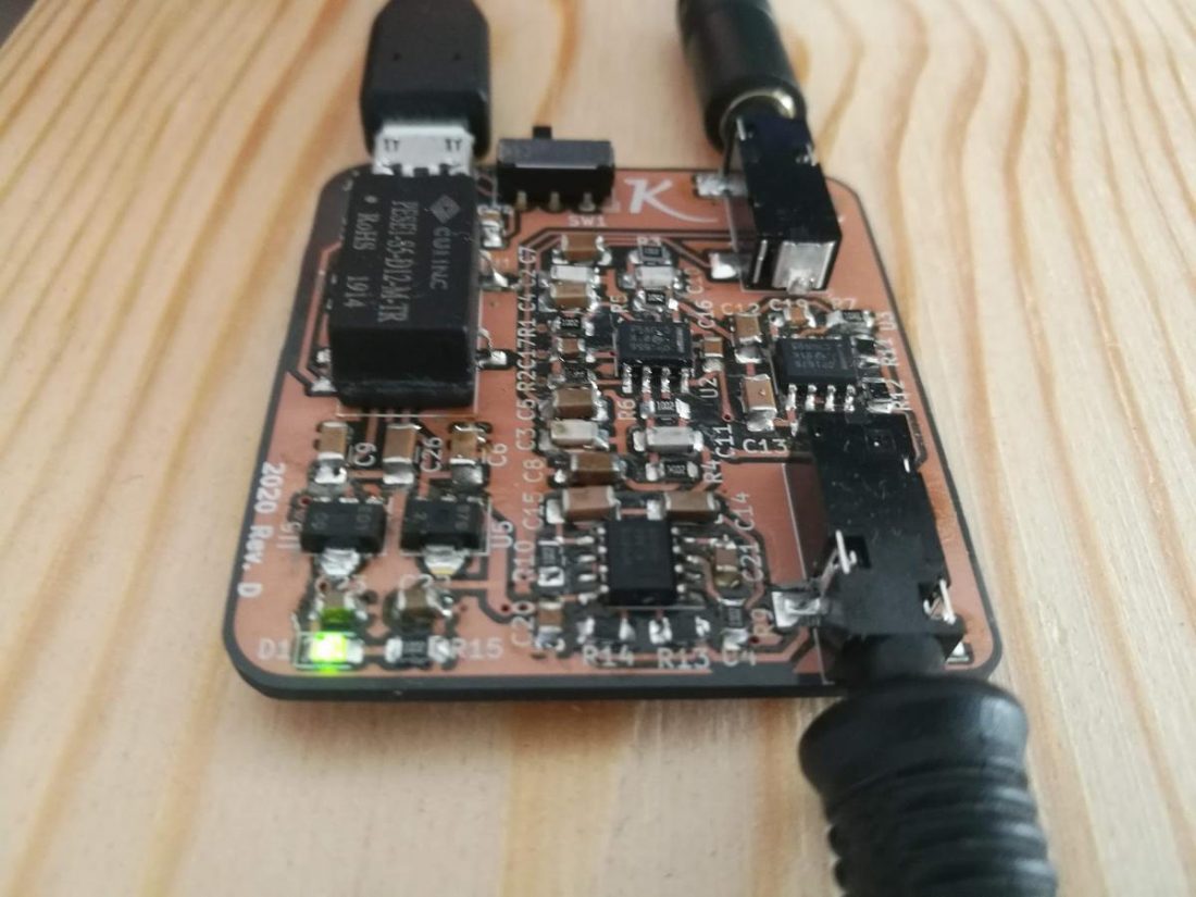
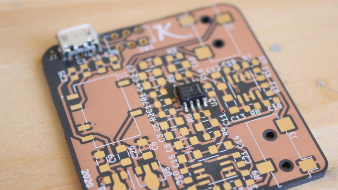
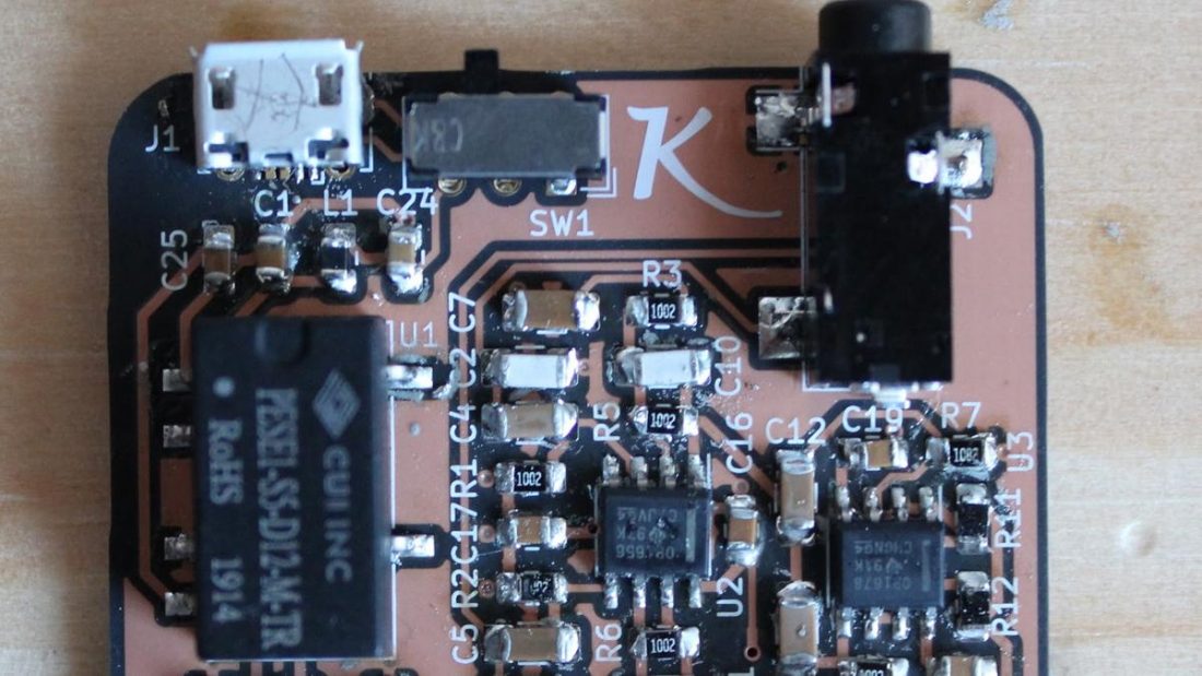
The NS-01 is a small DIY headphone amplifier. It is not the simplest possible project, since it was designed with size and performance in mind. The version presented here should be able to output 90 mA at 7 volts RMS, and work with even low-impedance headphones.
To keep the physical size small, the board is designed using surface mount components. These are rather small, so some care is required not to lose any parts inadvertently, but the assembly itself should be relatively straightforward. For the sake of simplicity, the part count is kept minimal. For example, the default configuration uses only two different resistor values.
The amplifier itself is composed of two stages:
- a voltage amplification stage,
- a buffer stage.
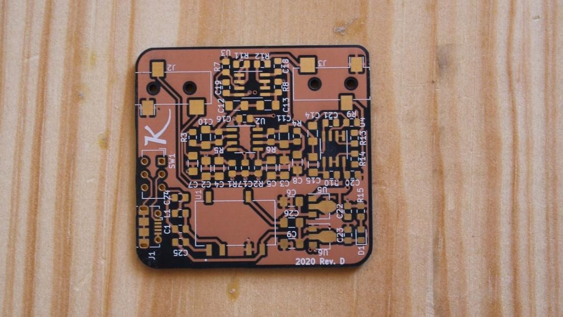
This two-stage approach should in theory improve the distortion performance, as the same device doesn’t have to deal with both voltage and current amplification. The rest of the circuitry makes up the power supply. The board shown here is revision D. Later revisions may introduce small changes, but the overall structure should remain the same.
There is a lot of talk among the hobbyist community about how SMT/SMD is difficult to use, but my personal experience is that SMT is actually easier to assemble by hand than through-hole components. The biggest obstacle is the size of the components, but that can be helped simply by using a magnifying glass or a microscope. To keep things simple, the smallest components in NS-01 are in 0805 size, or 2.0 x 1.2 mm.
Methods of Soldering
There are many different methods for soldering SMD components. Some are easier to do but might require specialized equipment. Most of these use solder paste, which is essentially a sticky paste made of tiny solder balls and flux which helps the molten solder to flow. From easiest to most difficult method:
Reflow oven
From converted toasters to large industrial systems, these heat the board until the solder paste melts and surface tension pulls the components in place. The board is cooled in a controlled manner to prevent the solder joints from becoming brittle.
Hot plate / skillet
Basically a poor man’s version of the reflow oven. The circuit board is heated from underneath until temperature is high enough to melt the solder and reflow the components. Cooling the board is difficult to control. The fact that the glass fiber material circuit boards are made of is a good thermal insulator makes this method inefficient as well. The initial heating period is rather long and nothing happens, and then suddenly everything happens at once.
Hot air reflow station
Blows hot air to heat the components and melt solder paste. Hot air stations are excellent when small fixes are needed, since you can focus the heat on a small area, unlike with an oven, but you can heat the whole component at once, unlike with an iron. Unfortunately, the airflow can move small components around, so care is required.
Soldering iron
The old-fashioned way of doing things. Takes more effort to produce pretty results. Only method able to work with solid solder. Even a cheap iron is enough, but make sure it’s temperature-controlled.
For the oven and hot plate methods, place all components first before heating. With the hot air method, work in small groups of components, and with soldering iron, place only a few components at a time so that you’ll have room to work in.
To place a component, put a tiny blob of solder paste on each of the pads on the PCB, and put the component in place with tweezers. Depending on the size of the component, it can be a good idea to hold the component gently down when soldering with an iron.
In this guide, I will be using a soldering iron and solder paste. Partly because I want to show how it’s done the “hard way”, but mostly because those tools are what I have easy access to.
Guide to Building Your Own Headphone Amplifier
- Things You Will Need
- Order of Soldering
- Step 1: USB connector
- Step 2: Gain stage
- Step 3: Buffer stages
- Step 4: Power
- Step 5: Cleaning up
Things You Will Need
Here is a short list of tools and parts required for the build. There are many alternatives and several suppliers, so take the following list only as a suggestion. If you’re not planning on building more electronics, it is worth considering borrowing the tools or visiting a makerspace.
Tools
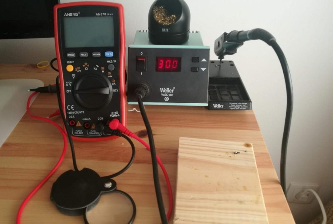
- Soldering iron. As long as it’s temperature-controlled, you’ll be fine. I use my 20-year old Weller, but TS100 has gotten good reviews.
- Solder paste. I used this ChipQuick product, but other brands work just as well.
- Multimeter. As long as it can measure resistance and voltage, you should be fine. For example, ANENG has decent inexpensive models.
- Tweezers (non-magnetic). Straight or curved depending on your preference.
- Loupe or microscope for inspection
- Rubbing alcohol
Components
Below is a list of suggested electronic components. There are several distributors, but for the sake of clarity I have added link only to one. Also in the case of resistors and capacitors etc. it is possible to replace them with another product as long as the value and packaging match. Sometimes distributors run out of stock on certain items, so sometimes finding alternatives is recommended.
| Description | Quantity | Link | Price (approx.) |
|---|---|---|---|
| NS-01 circuit board | 1 | Tindie | $10 |
| Operational amplifier, OPA1656 | 1 | Mouser | $2.95 |
| Operational amplifier, OPA1678 | 2 | Mouser | $1.66 |
| DC/DC converter | 1 | Mouser | $4.28 |
| Audio jacks | 2 | Mouser | $1.80 |
| Voltage regulator, positive | 1 | Mouser | $0.70 |
| Voltage regulator, negative | 1 | Mouser | $0.90 |
| LED (optional) | 1 | Mouser | $0.28 |
| USB connector | 1 | Mouser | $0.43 |
| Switch | 1 | Mouser | $0.52 |
| Resistor, 10 kOhm | 11 | Mouser | $0.65 |
| Resistor, 1 Ohm, 0805 | 4 | Mouser | $0.40 |
| Capacitor, 2.2µF, 0805 | 2 | Mouser | $0.54 |
| Capacitor, 1nF, 0805 | 1 | Mouser | $0.44 |
| Capacitor, 100nF, 0805 | 6 | Mouser | $0.60 |
| Capacitor, 1µF, 1206 | 11 | Mouser | $0.74 |
| Capacitor, 68pF, 1206 | 4 | Mouser | $0.84 |
| Capacitor, 4.7µF, 0805 | 2 | Mouser | $0.38 |
| Inductor, 6.8µH, 0805 | 1 | Mouser | $0.14 |
| $28.25 |
Do note that the quantities above are the components populated in the completed amplifier. Sometimes mistakes happen, so it may be wise to purchase an extra component or two. For several regions the distributors also offer free shipping if your order is large enough, so check if they have anything you want you can use to pad your order. I often buy different color LEDs and various audio connectors.
Order of Soldering
The order in which components are best soldered differs considerably between SMD assembly and through-hole assembly. Traditionally integrated circuits have been the last components to solder, but with surface mount, ICs should be some of the first components you mount. This is because ICs tend to be flatter and wider than most other components, and therefore it is easier to mount them first.
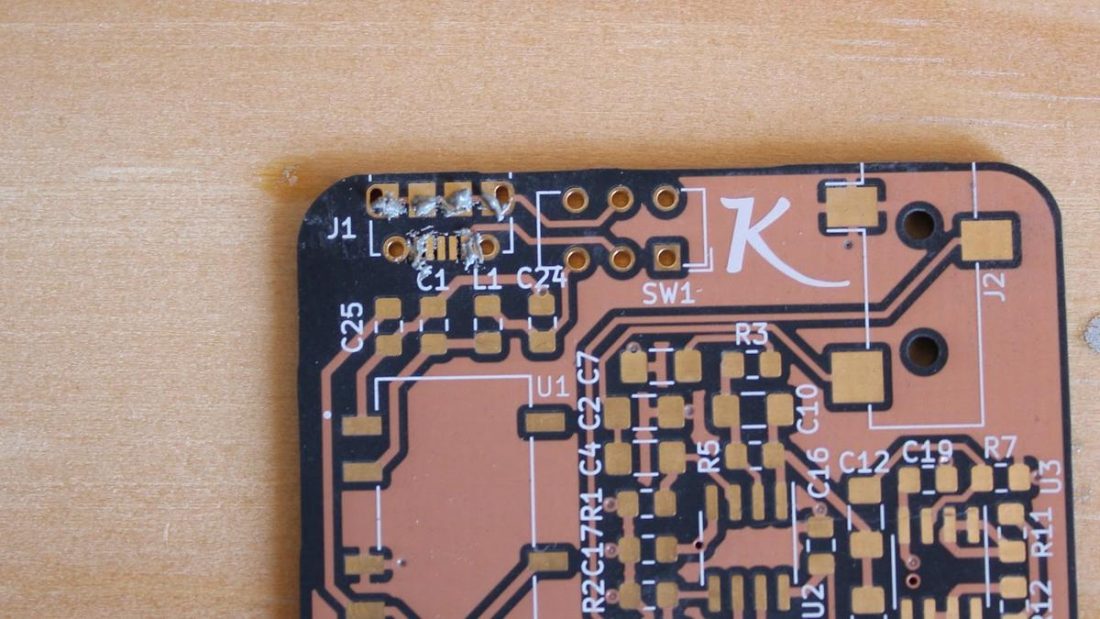
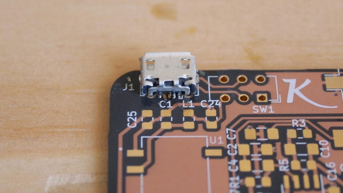
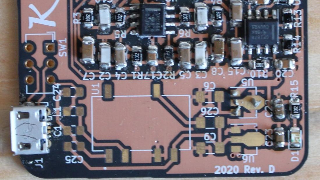
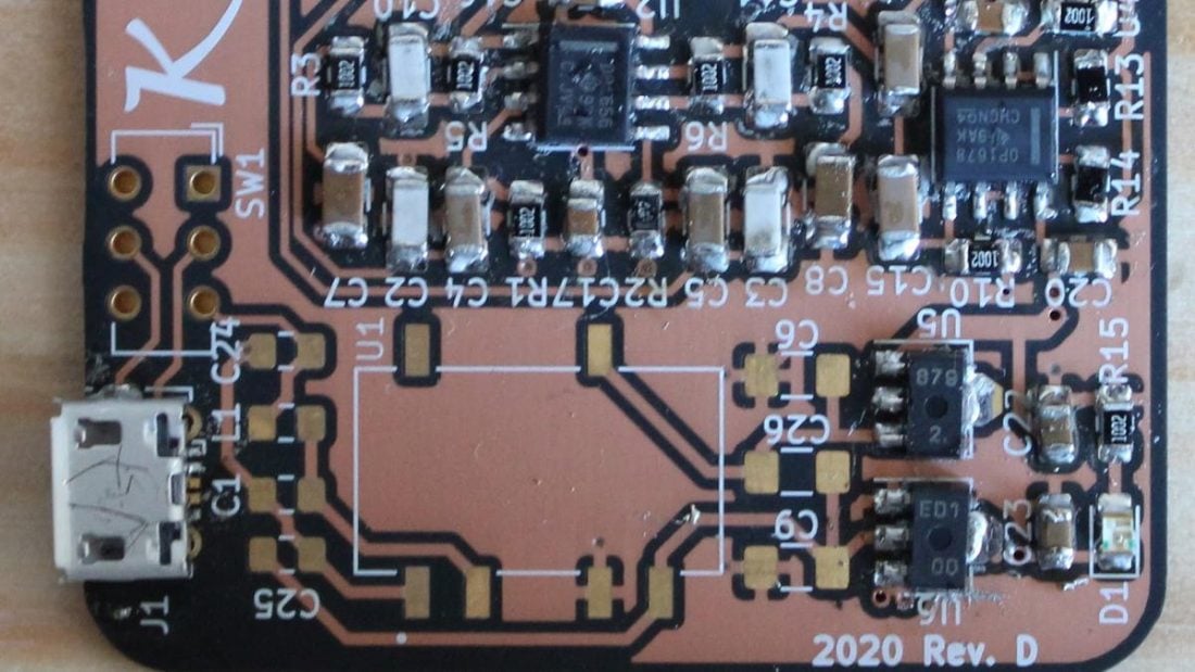
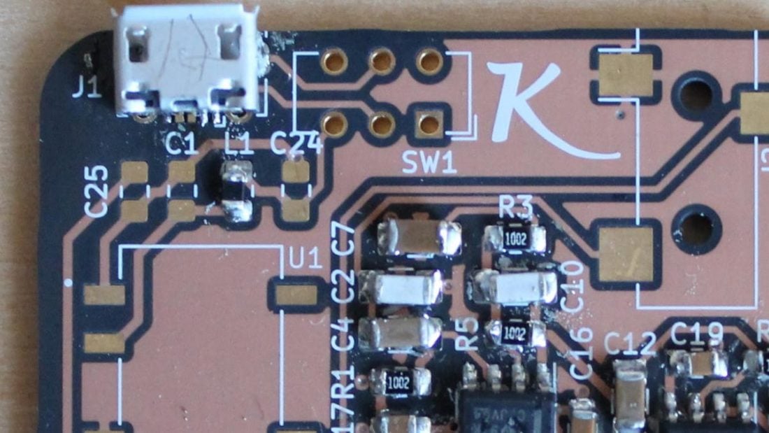
Step 1: USB connector
The NS-01 uses a micro-USB connector for power input. The connector is the trickiest part of the build, so it’s a good place to start. I place a tiny bit of solder paste on the pads, or if using solder wire, pre-tin the pads with as little solder as possible.
Once the connector is soldered, I check for shorts between the power pins with a multimeter. If there is no short circuit between the central pins of switch SW1, everything is good and the build can proceed. If the pins are shorted together, check the soldering and measure again. In the worst case, remove the connector and solder it on again.
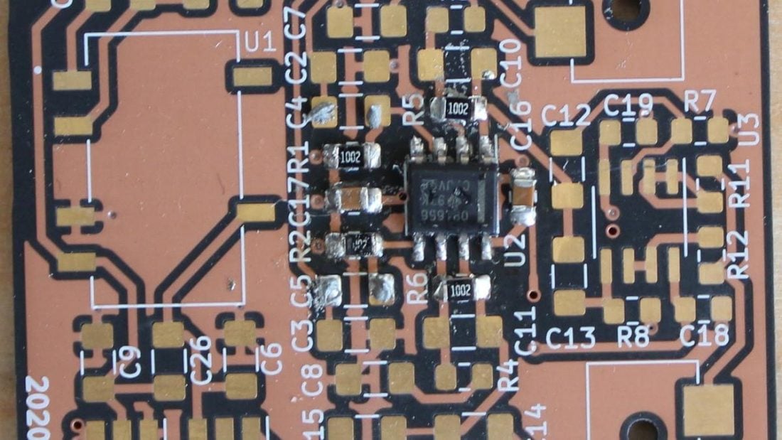
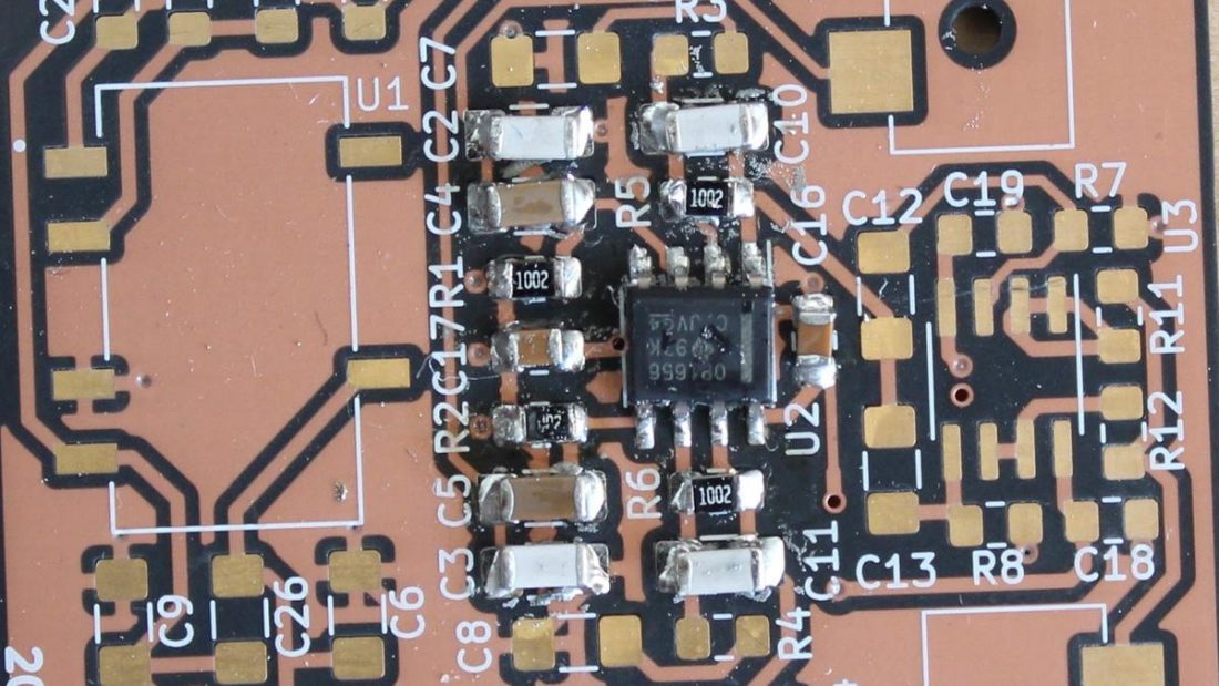
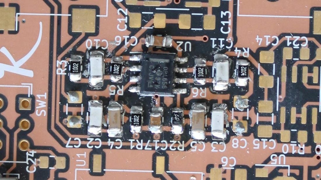
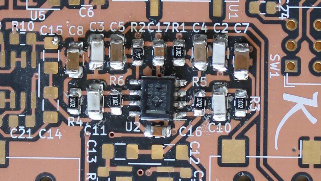
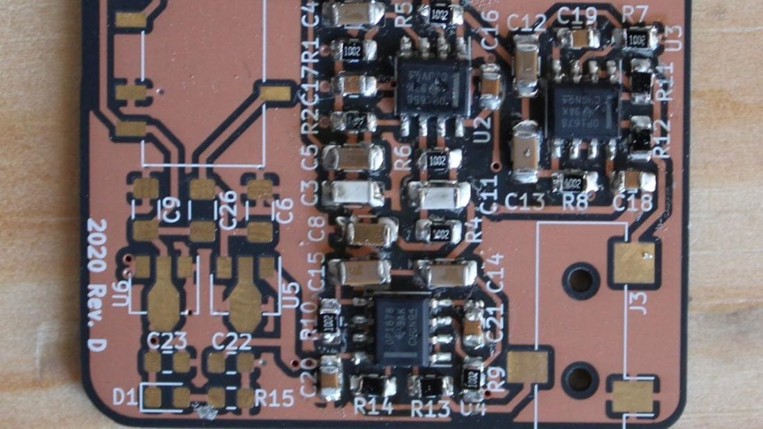
Step 2: Gain stage
After the power connector is safely mounted, I’ll start with the gain stage, because it’s the most central part of the board, and has the most components to it.
The gain stage takes the input signal and amplifies it, increasing the voltage level of the audio signal. In other words this stage applies gain to the signal. It also performs some filtering to remove noise from the signal that could disturb the system, such as radio frequencies. The amplification is performed by a OPA1656, which is actually two operational amplifiers in one package, one of them is used for the left and the other for the right channel.
I begin by placing the operational amplifier (op-amp) [U2], making sure the orientation is correct. Sometimes for ICs it’s easiest to use a method called drag soldering, but for these op-amps the pin pitch is large enough that it’s easy to solder one pin at a time. I hold the IC gently down with tweezers, pick one of the corner pins and solder it. Then I solder the opposite corner, and then the rest of the legs.
It’s never a bad idea to check that none of the pins are shorted before proceeding. If you used too much solder paste, it may have flowed under the component and might cause problems.
Next I add the decoupling capacitors [C16, C17]. These are 100nF 0805 capacitors, so be careful not to get them lost. These capacitors serve to smooth out the power supply for the op-amp and work as an energy reservoir in case of sudden demand. Without them, there is an increased risk that the op-amp would begin oscillating.
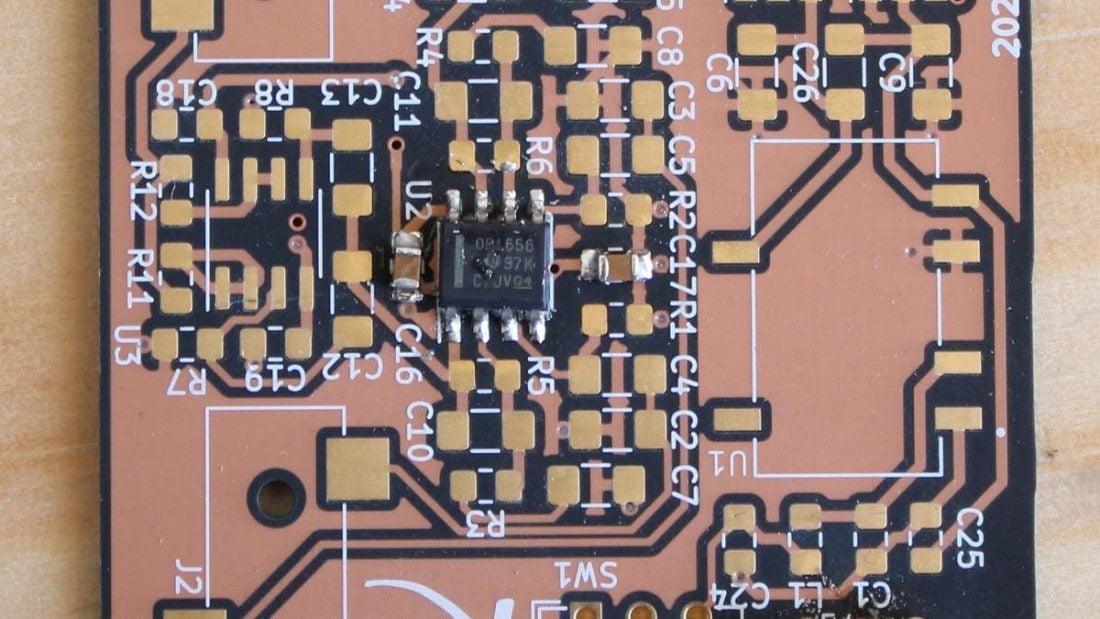
Next are the resistors [R1, R2, R5, R6]. These are all 10 kOhm 0805 resistors. After them, solder in 1µF 1206-size capacitors [C4, C5], followed by four 68pF capacitors [C2, C3, C10, C11].
The 68pF capacitors form two different lowpass filters for each channel, one at the signal input and the other in the feedback loop. The input filter prevents radio-frequency noise from entering the amplifier, and the feedback filter limits the amplifier bandwidth, reducing overall system noise.
The corner frequency (the frequency at which the filter causes the signal level to be -3 dB) of the feedback filter is about 230 kHz. It could be adjusted lower by increasing the capacitor value, but I wanted to use the same component as in the other filter, and I didn’t want to hear any complaints that the amplifier is “rolling off the high end”.
The 1 µF capacitors form highpass filters on each channel input, blocking off possible DC bias in the input signal, as well as reducing subsonic rumbling. The corner frequency of this high pass filter is 16 Hz.
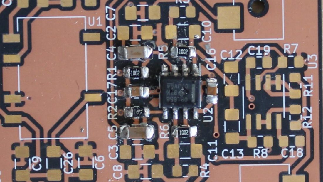
Next I install 10 kOhm resistors [R3, R4], followed by 1 µF capacitors [C7, C8]. The resistors form the feedback loop with [R5 and R6], and the capacitors create high-pass filters, reducing amplifier gain at DC to unity. This filter also has 16 Hz corner frequency.
The amplifier gain is determined by the ratio of R3 and R5 for the left channel and the ratio of R4 and R6 for the right channel. Because all of these resistors are of equal value, the amplifier gain is 2, or +6 dB. It is possible to adjust the ratio of the resistors for desired gain, but care should be taken to keep the maximum amplified signal below the operating voltage of 10 volts.
For my use, 6 dB is more than enough gain with modern sources, but your needs may be different. Do note that adjusting the gain also affects the corner frequencies of all these filters, so adjusting the capacitor values may be required.
Consumer line level however has a peak amplitude of 0.447 volts, allowing maximum gain factor of 22, or 20 to play it safe. This is however probably too loud to listen on most headphones.
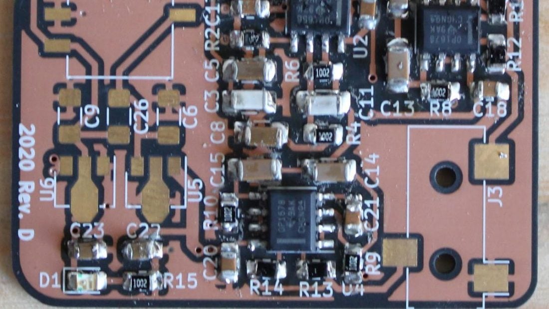
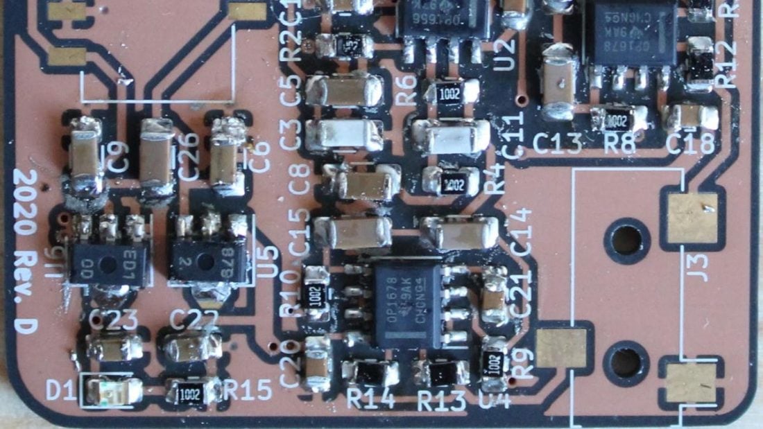
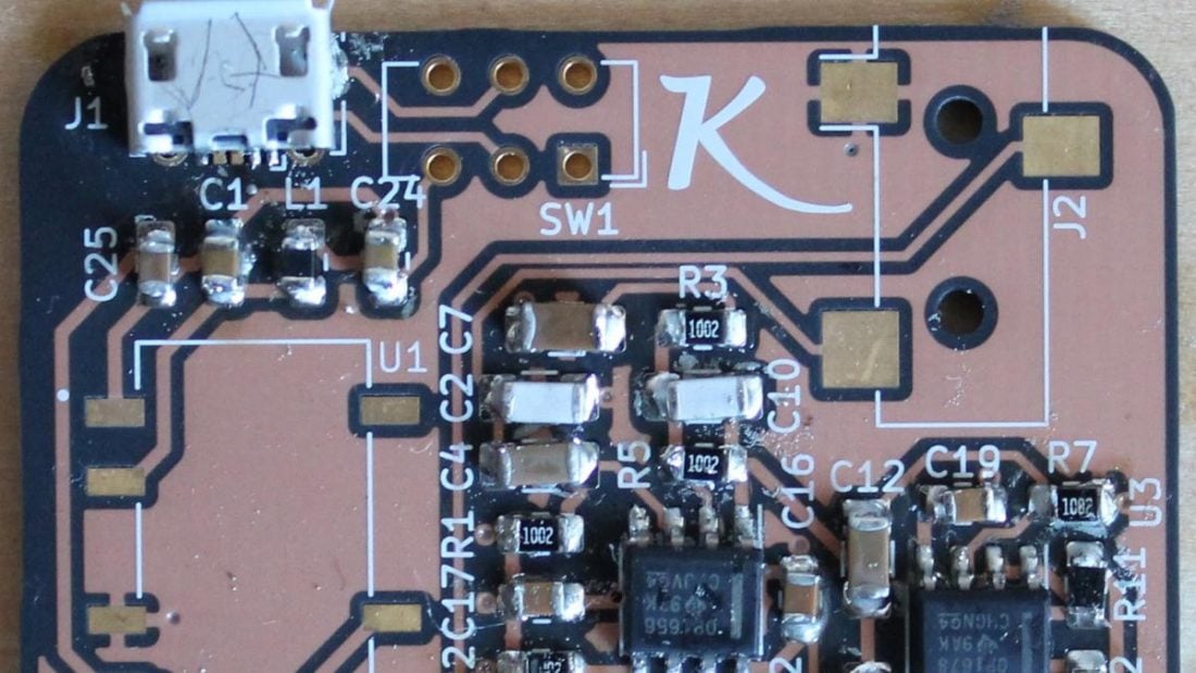
Step 3: Buffer stages
The buffer stage takes the amplified signal from the gain stage and sends it off to headphones. In essence it is an amplifier with a gain of one. Thus it provides no voltage gain, but it can provide current gain. This becomes important especially when using low-impedance headphones.
Each channel has its own buffer stage with 2 parallel op-amps (one full IC package per channel). Parallel op-amps means that the amplifier can provide more current to the headphones than a single op-amp could.
Because the sections are identical, they are easy to assemble simultaneously
Again I’ll start with the ICs [U3, U4].
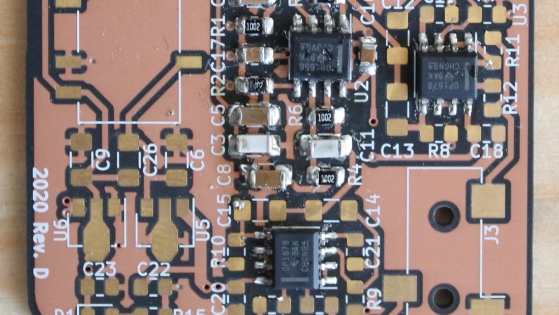
Next in line are capacitors [C12, C13, C14, C15]. These work as DC blockers, removing any bias that the voltage gain stage might have created. They’re functionally identical to [C4, C5] in the gain stage. These can be also replaced with zero-ohm links, but this should be only done if you are fairly sure that the input op-amp doesn’t introduce significant bias.
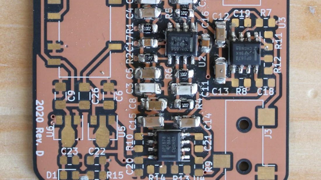
Next are 100nF op-amp decoupling caps [C18, C19, C20, C21], followed by resistors [R7, R8, R9, R10] which provide the ground path for the buffer amplifiers.
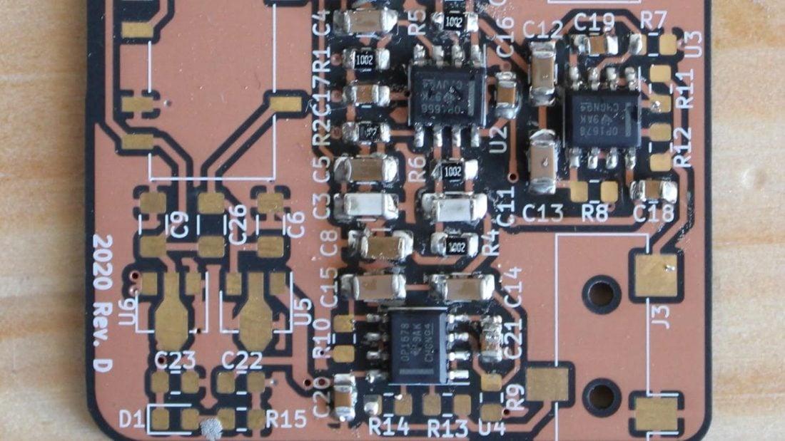
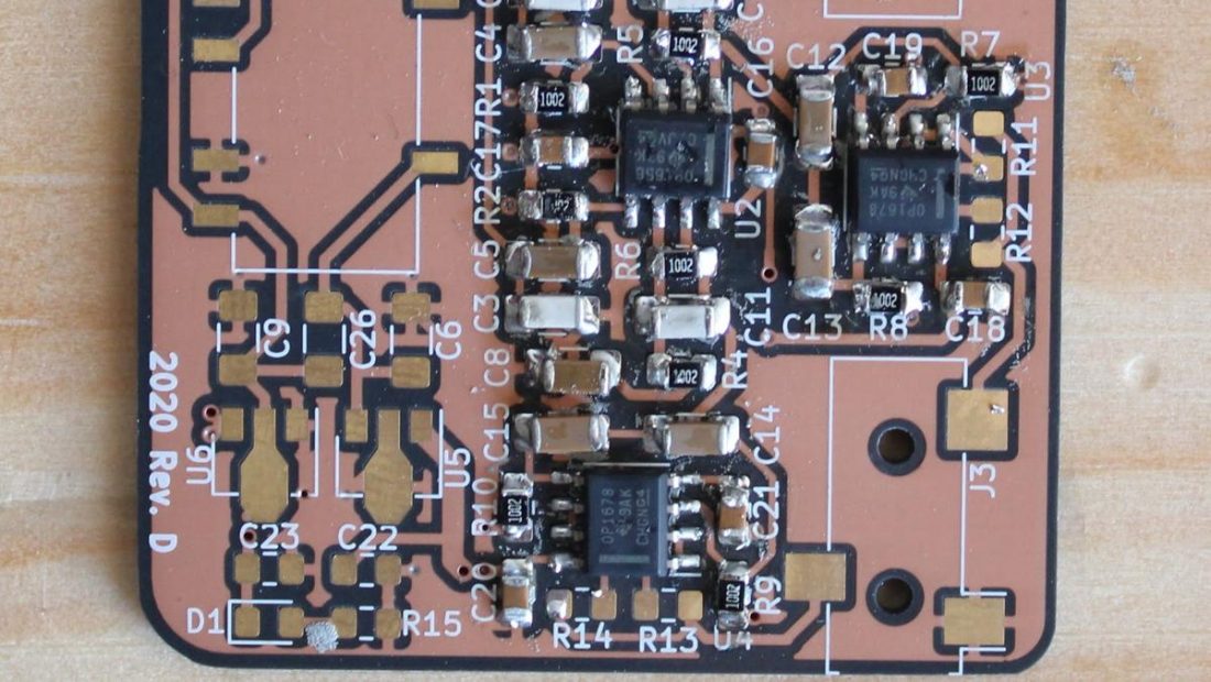
Final components in the buffer stage are the 1 ohm output resistors [R11, R12, R13, R14]. These help balance small differences in the buffer stages, and ensure that the op-amps aren’t trying to drive each other.
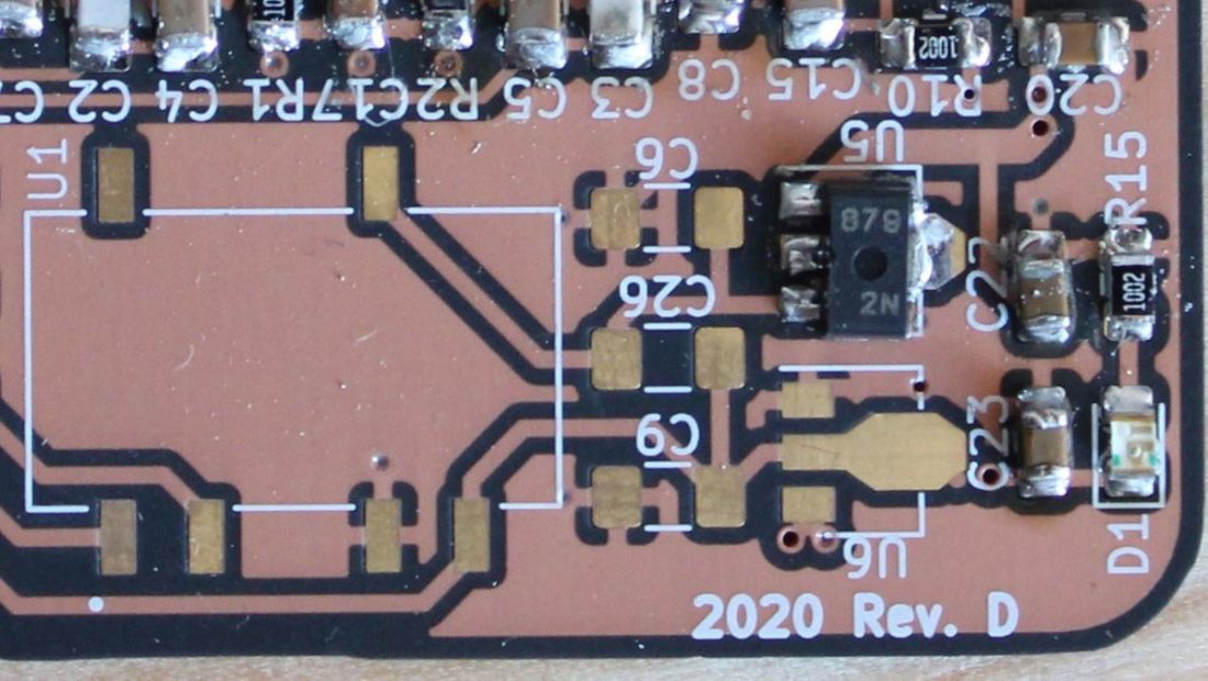
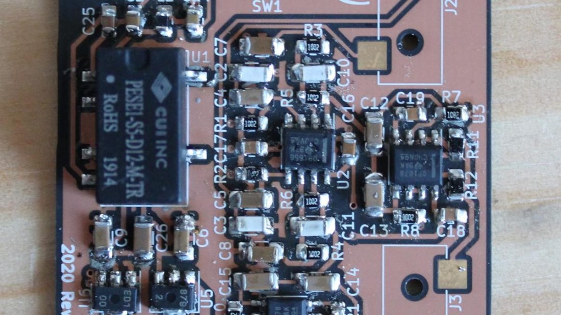
Step 4: Power
When the signal path is ready, it’s time to tackle the power section. I’ll start with the indicator LED [D1] and it’s limiting resistor [R15]. In my experience the nominal current of 20 mA usually makes LEDs all too bright. The idea is to indicate that the device is on, not to light up the room.
R15 is 10 kOhm, which is quite a high value, but because the LED is connected to the -10V power rail, it limits the current flow to about 1 mA, which should be enough. A lower value for R15 gives a brighter LED. Anything above 1 kOhm should work well. Or if you don’t need indication, you can leave D1 and R15 unpopulated altogether.
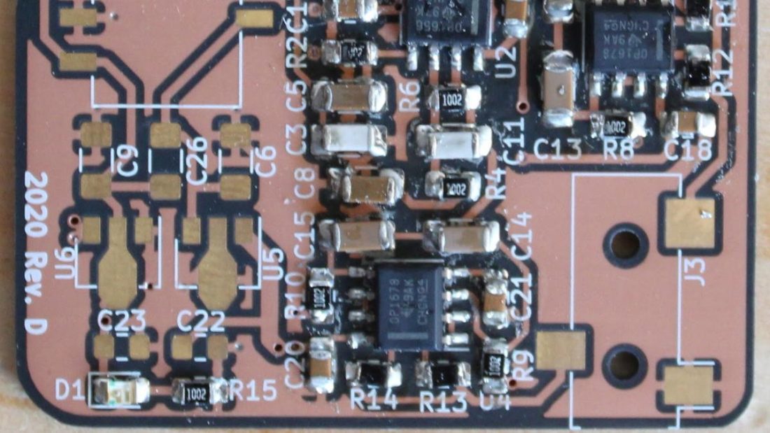
After the indicator, I populate the power supply capacitors [C22, C23]. These 2.2µF capacitors work as energy reservoirs and keep the voltage regulation stable.
Now it’s time to place the low-dropout linear voltage regulators (LDOs). I start with the positive rail regulator [U5], following it with the negative voltage counterpart [U6]. These are different components with different pinouts, so be careful not to swap them.
Next come the three decoupling/power filtering capacitors [C6, C9, C26]. Soldering these 1µF caps should be routine by now.
It is quite easy to put too much solder paste on the pads and cause a short in the LDO, so check with a multimeter. I made that mistake, and had to replace one of the LDOs. Fortunately I had bought spare components, because they are easy to break while trying to fix things.
I’ll leave the DC/DC converter [U1] for later due to its large size, and instead solder the rest of the components first.
Starting from the innermost component in the line of four footprints, I place and solder the inductor [L1]. This filters the incoming current and removes noise from the power supply. Then I install the 4.7µF capacitors [C1, C24]. Finally I solder in the 1nF capacitor [C25]. These four components are part of the DC/DC converter EMI filtering.
Now it’s time to solder the converter [U1]. The package is higher than the rest, but finding the correct angle for soldering the pads should not be difficult.
After the converter, I solder the input and output jacks [J2, J3]. When buying components, the type without switch used in this circuit (SJ-3523-SMT-TR) was out of stock, so I used the model with switch (SJ-3524-SMT-TR), and bent the extra legs up with pliers, so they wouldn’t touch other components [C19, R6].
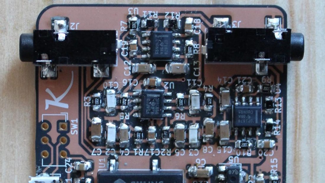
Power switch
Last is the power switch [SW1]. This is best put in last because it is a through-hole part, and the legs may cause the board to wobble after installing (depending on the surface). If you prefer to have the device always on you can wire the connections permanently. Connect the center pad of both rows to the pad closest to the usb connector. The pads on the input jack side are not connected and can be ignored.
Step 5: Cleaning up
After everything is soldered together, it’s time to clean the board up. I use isopropanol and a soft brush or cotton bud to remove flux and solder paste residue from the board. Denatured alcohol also works as a replacement for isopropanol, it’s just not as nice to use, and might leave some residue on the board. Don’t use acetone or other solvents, they may damage the components.
Then I use the multimeter to make sure there aren’t any short circuits between power rails. An easy way to do this is to measure the resistance across capacitors C1, C6, C9, C22, C23, C24, and C26. Due to capacitor action, the meter shows the resistance changing while measuring, but it should never be lower than about half a megaohm (the value rises as capacitors get charged).
Measure also the resistance between left and right channels and between each channel and ground, for both input and output. These should all read as open circuits, or at least have high resistance.
With no shorts in the circuit, I plugged the USB cable in and turned the switch on. The indicator LED will lit up. I used the multimeter to check all voltages, and everything was ok. VCC should be +10 and VEE -10, with 20 volts between pins 4 and 8 of each IC.
I plugged in a signal source with volume minimized. Finally, I plugged my headphones in ( use an expendable pair if you can, just in case anything goes wrong), and increased the volume.
A new headphone amp is ready.
Is there a schematic?
Hi Rudy,
A full schematic is included with the PCB from Tindie, but it’s not publicly available. This is so that I could recover some of the development cost.
I would buy one if I could look at the schematic to see what I’m paying for first…
Hi. The schematic is now on the Tindie page.
Schematic not publicly available – hmm, now that is suspiciously scary, because I hate dealing with ‘magical proprietary’ circuitry. I visited Tindie site no schematic. At least scheme w/o values – please, it would be really appreciated when we deal with DIY kit. Most good DIY projects provide some.
Can we buy this pcb & schematic ?